How Can PCB Achieve "Intelligent Transformation" in the AI Wave?
Against the backdrop of the rapid development of science and technology, the advent of the artificial intelligence (AI) era has brought a huge impact on various industries. The printed circuit board (PCB) industry, as an important pillar of the electronic ecosystem, is no exception. With the penetration of artificial intelligence in all aspects of life, from smart home devices to advanced data centers, the demand for high-performance PCBs has reached an unprecedented level.
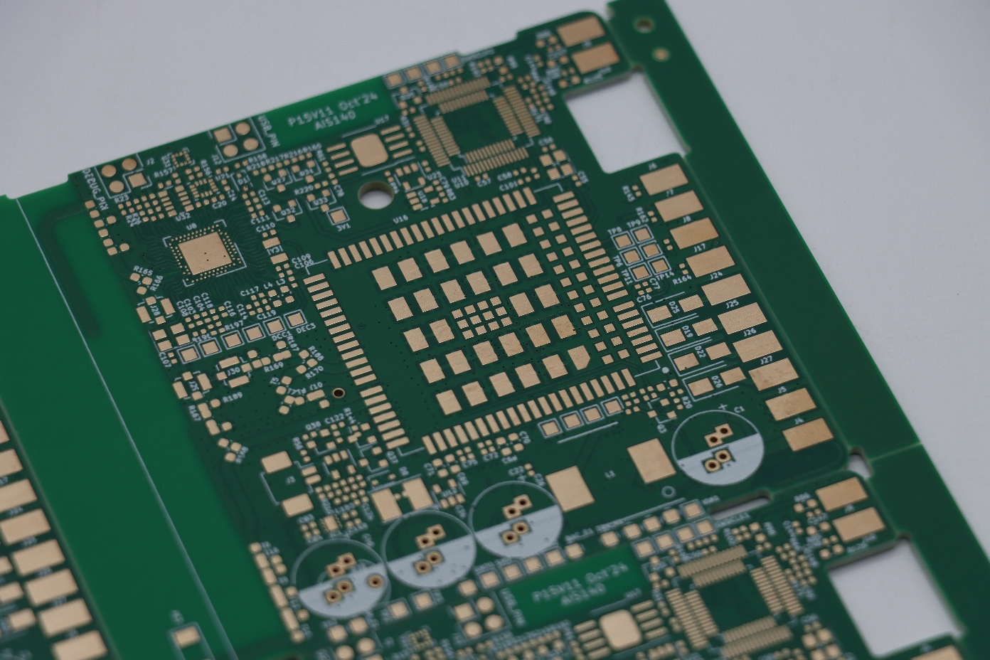
In particular, AI servers have become an important force driving the transformation of the PCB industry. These servers are specially designed to cope with the huge computing needs of AI algorithms and have extremely high performance requirements for PCBs. Among them, meeting the demand for high-speed signal transmission is one of the main challenges. AI applications generate and process massive amounts of data in real time, which requires PCBs to transmit signals at an extremely fast speed with minimal signal loss and interference.
To solve this problem, PCB manufacturers are adopting innovative materials and design technologies. High-frequency materials with low dielectric constants and low loss factors are more widely used to reduce signal attenuation. In addition, advanced wiring strategies such as differential pair routing and impedance matching are also playing a role in ensuring optimal signal integrity. These efforts have significantly improved the performance of Advanced PCB, enabling it to keep up with the ever-growing data rate requirements of AI applications.
Another area where artificial intelligence has a profound impact on PCB design is high-density interconnect (HDI). As the complexity of AI systems continues to increase, the demand for more compact and efficient PCBs is also growing. HDI technology achieves the integration of more components in a smaller space by using smaller vias, finer wires and multi-layer structures, thereby reducing the overall size and weight of the system.
AI-driven design tools are also revolutionizing the PCB design process. These tools use machine learning algorithms to analyze large amounts of data and optimize the layout and wiring of components. Taking into account factors such as signal integrity, power distribution and thermal management, these tools can generate more efficient and reliable PCB designs in a short time, which is much faster than human designers. This not only speeds up the design cycle, but also reduces the error rate and high rework costs.
In addition to design challenges, PCB manufacturers also need to optimize their production processes in the face of the growing demand for high-performance PCBs. In this regard, artificial intelligence also plays a key role. Machine learning algorithms can be used to analyze production data and identify areas for improvement, such as reducing waste, improving quality control and optimizing supply chain management.
For example, AI-driven quality control systems can detect defects in PCBs more accurately and quickly than traditional methods. The Automated Optical Inspection (AOI) system we use uses computer vision and machine learning algorithms to analyze PCB images and identify any anomalies or defects. This enables us to quickly detect and solve problems, thereby improving the overall quality of products and reducing rework costs.
In addition, artificial intelligence can also optimize the supply chain by predicting demand, managing inventory and coordinating with suppliers. By analyzing historical data and market trends, AI algorithms can accurately predict the demand for PCBs, enabling manufacturers to plan production schedules and inventory levels more effectively. This helps reduce costs, improve efficiency and ensure a stable supply of high-quality PCBs.
As the PCB industry continues to adapt to the needs of the AI era, PCBgogo is at the forefront of this transformation. As a leading PCB manufacturer, we quickly embrace the latest technologies and trends in the industry. Through investment in research and development, we have successfully developed innovative solutions that meet the high-performance requirements of AI applications.
Our dedication to quality and innovation is reflected in our advanced manufacturing facilities and high-quality team of engineers. The company uses the latest manufacturing technologies, such as the aforementioned Automated Optical Inspection (AOI) and X-ray inspection, to ensure the highest level of quality control. In addition, our engineers are constantly exploring new materials and design technologies to improve the performance and reliability of PCBs.
In conclusion, the AI revolution has brought both challenges and opportunities to the PCB industry. By leveraging the latest technologies and trends, PCB manufacturers can meet the high-performance requirements of AI applications and drive industry innovation. Companies like us, PCBgogo, are leading this transformation, fully demonstrating the importance of embracing change and investing in research and development. As the demand for AI-driven devices continues to grow, the PCB industry will play a key role in driving the next wave of technological innovation.