
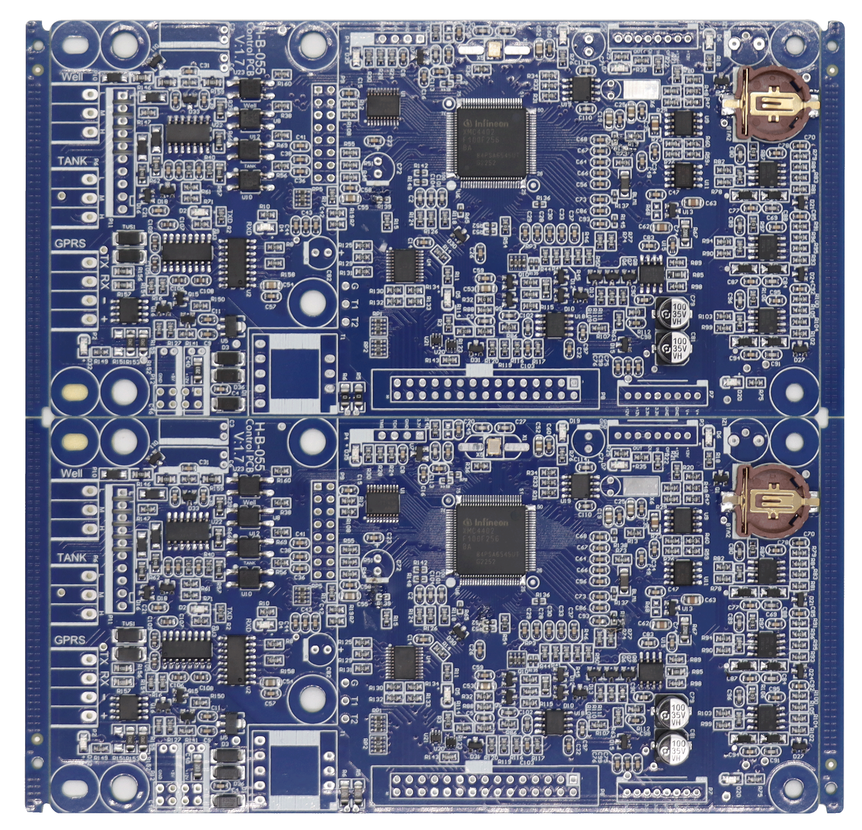
From Bare Board to Brain: A Deep Dive into PCB Assembly (PCBA)
A bare printed circuit board (PCB) is just a piece of fiberglass and copper, an empty canvas waiting for a purpose. Its journey to becoming the "brain" of an electronic device—a PCBA, or Printed Circuit Board Assembly—is a meticulous process that transforms passive materials into a functional, complex circuit. This isn't just about soldering components; it's a high-stakes dance of precision, automation, and quality control that ensures your phone, laptop, or car works exactly as it should, every single time.
While the design phase lays the blueprint, the assembly process is where the magic truly happens. It's an intricate sequence of steps, each one critical to the final product's reliability.
1. The Solder Paste: The Board's Lifeblood
The first step in assembly is applying a solder paste, a mixture of tiny metal solder balls and a sticky flux. This paste acts as the temporary glue that holds components in place before soldering and provides the final electrical connection.
Solder Paste Inspection (SPI): Before a single component is placed, the solder paste application is checked using a sophisticated SPI machine. This machine uses 3D imaging to verify that the paste is applied with the correct volume and thickness. A tiny error here—a blob too big or a dab too small—can lead to short circuits or poor connections down the line, so this step is non-negotiable for high-quality assembly.
2. The Pick-and-Place Machine: The Robotic Artisan
Once the solder paste is perfect, the board moves to the Pick-and-Place (PnP) machine. This is where automation truly shines. A PnP machine is an incredible piece of engineering that can place thousands of tiny components per hour with astonishing accuracy.
Component Placement: The machine uses a vacuum nozzle to "pick" components from feeders and "place" them onto the solder paste on the board. With component sizes shrinking to fractions of a millimeter, the precision of these machines is paramount. For complex devices, like a modern smartphone, a single board might have over a thousand components, and a single misplacement can render the entire board useless.
Challenges with BGAs: For components like a BGA (Ball Grid Array), where the connection points are tiny solder balls on the underside of the chip, placement is even more critical. There's no way to visually inspect the connections after placement, so the machine’s accuracy must be absolute.
3. The Reflow Oven: Fusing the Connections
With all the components placed, the board is sent through a reflow oven. This isn't your kitchen oven. It's a precisely controlled tunnel with multiple heating zones.
The Reflow Profile: The oven heats the board following a specific temperature profile. The first zone activates the flux in the solder paste, cleaning the connection pads. The next zone heats the board to the precise melting point of the solder. As the solder melts, it forms a strong electrical and mechanical bond between the component and the PCB pad. The final zone cools the board to solidify the connections. A correct profile is essential; too hot and you can damage components, too cool and you get "cold joints" that fail over time.
4. Final Inspection and Testing: The Gatekeepers
After the board comes out of the reflow oven, it undergoes a rigorous inspection process to ensure everything is perfect.
Automated Optical Inspection (AOI): An AOI machine uses high-resolution cameras to rapidly scan the board and compare it to a reference image. It can detect a wide range of defects, from missing components and wrong polarity to solder bridges and shorts.
X-ray Inspection: For BGAs and other components with hidden solder joints, an X-ray machine is used to look right through the component and verify the quality of the solder balls underneath.
In-Circuit Test (ICT) and Functional Test: The final steps involve testing the electrical functionality. An ICT checks for shorts, opens, and component values, while a functional test simulates the board's real-world operation, ensuring it performs its intended job.
Conclusion: Beyond the Board
The journey from a bare PCB to a fully assembled PCBA is a testament to modern engineering and manufacturing. It's a fusion of advanced robotics, precise thermal control, and rigorous quality assurance. At PCBgogo, we understand that this is more than a series of steps; it's a commitment to reliability. We don’t just manufacture boards; we deliver the "brains" of your products. Our investment in cutting-edge Pick-and-Place machines, advanced SPI systems, and comprehensive inspection protocols ensures that every board we assemble is not only correct but also built to last. For us, every PCBA is a promise of quality and performance, a crucial link in the chain of innovation that drives the modern world.

