
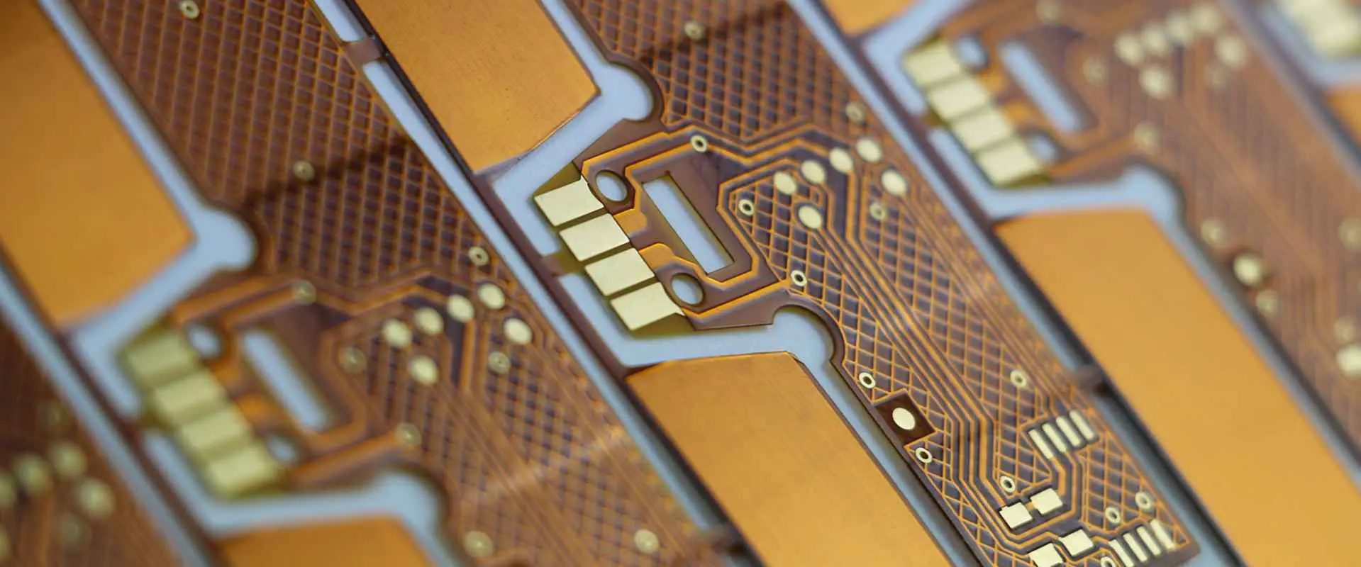
Exploring the World of Thin Copper Foil PCBs
In the ever-evolving PCB landscape, thin copper foil PCBs have emerged as quiet revolutionaries, especially as consumer demand pushes for electronics that are both smaller and more powerful. These specialized boards, with copper layers measuring 1/2oz or less (where 1oz equals approximately 35μm), are reshaping what’s possible in high-frequency and compact device design. Let’s take a closer look at their performance, advantages, real-world applications, and the latest industry shifts.
Performance Highlights
Top-Notch High-Frequency Performance
When it comes to signals above 10GHz, thin copper foil truly comes into its own, thanks to a phenomenon known as the skin effect. At these frequencies, electrical current tends to flow along the outermost layer of a conductor—think of it like water skimming the surface of a lake—with a 10GHz signal penetrating only about 2μm deep. This makes thin foils far more efficient: a 1/4oz foil (8.75μm thick) uses 22.8% of its material for actual conduction, compared to just 5.7% in a 1oz foil (35μm). The result? Less resistance and significantly reduced signal loss, critical for maintaining clarity in high-speed data transfer.
Adding to this advantage is the surface smoothness of thin foils. A 1/2oz rolled copper foil, for example, has a surface roughness (Ra) of around 1μm, while a standard 1oz electrolytic foil typically measures 3μm. This matters because rough surfaces scatter high-frequency signals: tests show a 10GHz signal loses just 0.1dB/cm in a low-roughness thin foil, versus 0.3dB/cm in a thicker, rougher alternative.
Precise Impedance Control
For high-frequency systems to work seamlessly, impedance—the resistance to signal flow—must stay consistent. Thin copper foils are more sensitive to small changes in line width, but modern manufacturing techniques like laser direct imaging (LDI) solve this challenge. For a 1/4oz foil with a 0.1mm line width, LDI keeps deviations within ±0.005mm, ensuring 10GHz signals maintain an impedance consistency (CPK 1.3) on par with thicker foils. This stability minimizes signal reflection, a common culprit in dropped connections or data errors.
Key Advantages
Cost-Effective for High Frequencies
While thin copper foil PCBs may cost a bit more upfront than standard boards, they prove their worth in high-frequency applications. By boosting communication range by over 10% and reducing signal degradation, they eliminate the need for extra amplifiers or signal boosters—saving money in the long run, especially in large-scale productions like 5G infrastructure.
Light and Compact
Every micron counts in devices where space is at a premium. Thin copper foils trim down PCB weight and thickness, making them ideal for portable gadgets, drones, and aerospace equipment. In smartphones, for instance, this slim profile frees up space for larger batteries or more advanced sensors. Even in flexible PCBs, thin copper enhances bendability—think of the curved screens in smartwatches—without weakening signal performance, a balance that’s hard to achieve with thicker materials.
Real-World Uses
5G and Fast Communication
5G networks, with their need for ultra-fast data transfer (up to 10Gbps), rely heavily on thin copper foil PCBs. They’re found in base station antennas, where they handle the high-frequency millimeter waves that enable 5G’s speed, and in smartphones, ensuring smooth streaming and low-latency gaming.
Car Electronics
Modern vehicles, especially those with autonomous features, depend on precise, high-speed data. Thin copper foil PCBs power radar systems that detect obstacles up to 300 meters away, using their stable impedance to ensure accurate distance calculations. They also support in-car Wi-Fi and vehicle-to-vehicle (V2V) communication, keeping drivers connected and safe.
Wearables
From fitness trackers to medical monitors, wearables demand PCBs that are lightweight, durable, and energy-efficient. Thin copper foils deliver on all fronts: their small size fits comfortably on the wrist, their high-frequency performance enables continuous Bluetooth syncing, and their efficiency extends battery life—so your smartwatch can last through a full day of workouts.
Industry Trends
Manufacturers are now developing new copper alloys that combine thinness with enhanced durability, making these PCBs even more resistant to heat and corrosion. 3D printing is also entering the fray, allowing for intricate, custom designs that maximize thin foil performance. Meanwhile, as flexible PCBs gain ground in foldable phones and medical implants, thin copper remains a key ingredient, enabling both flexibility and power.
PCBgogo's Take
At PCBgogo, we’re proud to be at the forefront of thin copper foil PCB innovation. Our production facilities are fine-tuned to control every detail—from copper thickness to surface smoothness—ensuring each board meets the strictest standards for high-frequency performance. Whether you’re building 5G equipment, next-gen car tech, or cutting-edge wearables, we work with you to craft custom solutions that fit your needs. By investing in R&D and staying ahead of material trends, we make sure our PCBs don’t just keep up with industry demands—they set new benchmarks. Choose PCBgogo, and let’s build electronics that redefine what’s possible.

