An Introduction to Electroless Nickel Immersion Gold (ENIG) by PCBGOGO
An Introduction to Electroless Nickel Immersion Gold (ENIG) by PCBGOGO
Electroless nickel immersion gold (ENIG) process has been widely used in PCB fabrication, which is an auto-catalytic process that is related to deposition of nickel on the palladium-catalyzed copper surface. And it will provide the appropriate concentration, temperature and pH levels necessary to create a consistent coating that need to replenish the reducing agent with nickel ions. The gold adheres to the nickel plated areas by molecular exchange during the immersion gold process to prevent the nickel from being oxidized until the soldering process arises. What’s more, the thickness of gold needs to meet the demands of certain tolerances so that make sure the nickel has a great solderability.

What’s electroless nickel immersion gold (ENIG)
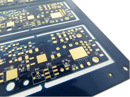
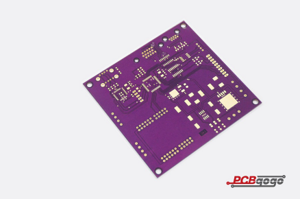
Electroless nickel immersion gold (ENIG) is a type of surface plating used for printed circuit boards, which is made up of an electroless nickel plating covered with a thin layer immersion gold, it’s mainly in protecting the copper from being oxidized or corroded on the surface of circuit board, as well as having a better soldering for the copper. Electroless nickel immersion gold is a RoHS complaint surface finish that offers a reliable solder joint, a planar surface, and is resistant to environmental storage conditions, handling and so on.
Advantages of electroless nickel immersion gold
Electroless nickel immersion gold (EMIG) is an expensive surface finish technology, but it’s still popular because of the following reasons:
1. ENIG complies with all RoHS requirements.
2. Electroless nickel immersion gold has some great chemical properties contributed by nickel; and gold layer, which are surface planarity, impressive wettability, and coplanarity, as well as long shelf life;
3. A nickel layer has two functions in ENIG. It plays an important role in stopping the interfusion between gold and copper. But it will react with tin to create intermetallic compound (IMC) Ni3Sn4, which has a great solderability;
4. The gold layer has the advantages of high strength, antifriction, low contact resistance and few chances of oxidation. And they are good to meeting the demand of PCB conductivity, as well as protecting the nickel and copper layers from being oxidized. What’s more, it does well in improving the solderability;
5. There are a great reflow cycle and it can work well without dummy plating. As well as is well-known as the electrical testability with good adhesion;
6. It’s good for plated through hole in PCB fabrication;
7. The gold plating is gold wire bondable, and make it easy to solder;
8. ENIG is best for fine pitch products as there is square-edged and flat for the tracks or pads

PCB fabrication with ENIG surface finish in PCBGOGO
With over 10 years as an industry leader, PCBGOGO is one of the most experienced PCB and PCB assembly manufacturer in China. highly specialized not only in quick-turn PCB prototype and PCB assembly, but also medium and small volume PCB fabrication. And we will try our best to meet your demands of PCB with ENIG surface finish and committed to adhering to the strictest standards in PCB fabrication and assembly.
If you have any questions, please feel free to contact us with service@pcbgogo.com, we will be happy to help you.

