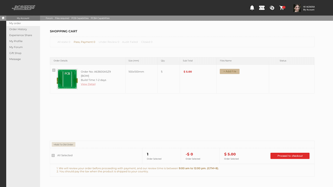
Instant Quote
Quick Order
+ Add Gerber File
Upload gerber file to read PCB parameters like the board size, hole, track/spacing.
Only accept .rar or .zip & Maximum 10M.
You have uploaded the file
successfully and please check the parameters
below. Well continue to check all the individual layers to make sure that
they recorrect
文件上传失败,请检查格式或网络是否正常,重新上传文件。
Failed image display, please check the file format or network, then upload again.
Because of the imperfect algorithm of our Gerber-to-Image tool, it may cause
inaccurate display of PCB images, which does not mean there is a problem
with the files. Whether your files is OK for production will be subject to our
final review results.eg:cut-outs lost;Image shown is a representation only.
Thickness
0.203
0.305
0.508
0.813
1.524
Unit: mm

Thickness
0.254
0.338
0.508
0.762
1.524
Unit: mm
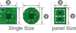
Different Design
in Panel

it means- we will charge extra panel costs when there are different
kinds in 1 PCB design. For same kinds, it needn't charge.
Size (single)
inch”↔mm
Inch”↔mm conversion
If you enter in units of inches and press the [Convert] button, it will be converted into units of millimeters in the quotation form.
Panel Way
Single piece
Panel by Customer
Panel by PCBgogo
The above panel way and panel size are for reference only which shall be subject to the review of our PCB engineer.
Panelization Detail:
Panel size:
0.00 X
0.00 mm
0 panels =
0 pcs individual PCBs
Image for panelized board ↓ (for reference only)
The final price will vary depending
on the paneling method and quantity.

The full board are by only one single board or be arrayed with the same or different PCBs
Layers
1 Layer
2 Layers
4 Layers
6 Layers
8 Layers
10 Layers
12 Layers
14 Layers
FR4-TG
GF212 TG 130
KB6165F TG 150
KB6167F TG 170
S1000H TG 150
Thickness
0.2
0.4
0.6
0.8
1.0
1.2
1.4
1.6
1.8
2.0
2.4
2.8
3.0
3.2
3.6
3.8
4.0
Unit: mm
Min Track/Spacing
3/3mil
4/4mil
5/5mil
6/6mil
8/8mil ↑

Min Hole Size
0.15mm
0.2mm
0.25mm
0.3mm ↑
0.8mm ↑
1.0mm ↑
No Drill

Solder Mask
Green
Red
Yellow
Blue
White
Purple
Black
Matte black
Matte green
None
Usually green color, the lead time will be longer if you choose other colors.
Gold Fingers
Yes
No
Bevelling
No
Yes (20°)
Yes (30°)
Yes (45°)

HASL with lead
HASL lead free
Immersion gold(ENIG)
OSP
Hard Gold
ENEPIG
Immersion silver(Ag)
None
*The above options are only Gold fingers Surface Finish
Thickness of
Immersion Gold
1U"=0.0254um
Au/Ni thickness
Au:10U"/Ni:120U"
Please choose other options of Gold /Nickel thickness here
1U"=0.0254um
Au:3U"/Ni:120U"
Au:5U"/Ni:120U"
Au:10U"/Ni:120U"
Au:15U"/Ni:120U"
Au:20U"/Ni:120U"
Au:25U"/Ni:120U"
Au:30U"/Ni:120U"
Please Enter | Au:
U"/Ni:
U"
Surface Finish
HASL with lead
HASL lead free
Immersion gold(ENIG)
OSP
Hard Gold
ENEPIG
Immersion silver(Ag)
None
Thickness of
ENEPIG
Ni:200U" / Pd:2U" / Au:2U"
Please choose other options of Au/ Pd thickness here
Ni:200U" / Pd:1U" / Au:1U"
Ni:200U" / Pd:2U" / Au:2U"
Ni:200U" / Pd:3U" / Au:3U"
Ni:200U" / Pd:4U" / Au:4U"
1U"=0.0254um
Thickness of
Immersion Gold
1U"=0.0254um
Au/Ni thickness
Au:3U"/Ni:120U"
Please choose other options of Gold /Nickel thickness here
1U"=0.0254um
Tick "Yes" to agree PCBGOGO to replace "HASL" to "ENIG" randomly because
of factory fabrication requirement.
Yes
No
Via Process
Tenting vias
Plugged vias
Vias not covered
Tips: If you use .PCB and .PCBDOC format file, we will fabricate the drills in PCBs as your selected options. This option is invalid if your file is Gerber file , as we will do according your Gerber file.
Finished Copper
1 oz. Cu
2 oz. Cu
3 oz. Cu
4 oz. Cu
5 oz. Cu
6 oz. Cu
7 oz. Cu
8 oz. Cu
9 oz. Cu
10 oz. Cu

Inner Copper
1 oz
1.5 oz
2 oz
3 oz
4 oz
5 oz
6 oz
PCB Assembly
The above PCBs need assembly service
SMD-stencil
Order together with PCB
+Additional Options
(Castellated holes ,Edge Plating ,impedance control, buried / blind vias,Custom Stackup,UL Marking)
Below options, their cost is not included in the online quotation
Peelable Soldermask
Coating material could be removed after board through wave soldering
Do not add PCB order number
Do not add PCB order number on board( extra +$1)
Half-cut/Castellated Holes
PTH holes or vias that are cutted through to create a partial or half hole to form an opening into the side of the hole barrel.Generally they are used for mounting a PCB to another one.
Edge Plating
The partial edge of the PCB plated with copper
Impedance control
The resistance to the flow of current, represented by an electrical network of combined resistance, capacitance and inductance reaction,usually in high-frequency circuits
Halogen-Free
Halogen-free PCB, it should have less than 900 parts per million of chlorine or bromine, with less than 1,500 ppm of total halogens.
Buried/blind vias
High-density multi-layer PCBs may have microvias: blind vias are exposed only on one side of the board, while buried vias connect internal layers without being exposed on either surface.
Custom Stackup
Apply to multilayer pcbs only.Stack-up refers to the arrangement of copper and insulating layers that make up a PCB before starting board layout design.
Carbon Mask
Carbon ink creates surface resistors and a protective contact surface for switches.
Via in pad
The microvias filled with non-conductive epoxy then capped and plated over
Via filled with resin
The microvias filled with epoxy
Countersinks/Counterbores
Countersink is a cone shaped hole in PCB for the tapered head of a screw. Counterbore is flat-bottomed hole and its sides are drilled straight down, usually used to fit a hex-headed cap or screw
Z-axis milling
A variable level elevation can be milled at the edge or within a circuit board. This is called Z-axis milling.
Confirm work file
work file is the Gerber file after PCBGOGO optimizes your PCB project, and we will have customers confirmed their work file, the lead time of your order will be counted by the time of work file confirmed
Other Special
Request
Your number will be added to the board. Kindly leave a note if you do not require this additional service.
SMD-Stencil
Order together with PCB
Stencil Side
Top
Bottom
Top+Bottom(On Single Stencil)
Top & Bottom(On Separate Stencil)
Thickness
0.10mm
0.12mm
0.15mm
0.2mm
Existing fiducials
None
Half lasered
Lasered through
PCB Assembly
The above PCBs need assembly service
Combo
You supply some parts we do the rest
Number of
Unique Parts
Fill in the exact quantity or 0 to wait for manually review.
Please enter the total number of single PCBs.(not the set number)
Number of
SMD Parts
Total quantity of SMD components for each board.
Number of
Through-Hole Parts
Total quantity of through holes components for each board.
Panel Way
Single piece
Panelized PCBs
If single pcb qty is more than 20pcs or the part solering points are less than 100,then we suggest do panel.Or we may charge extra wastage fee.
Assembly Side(s)
Are parts mounted on one side only, or both sides?
Conformal coating
Please contact your sales representative.
Detailed information
of assembly
Price does not include PCB fabrication or the cost of components, exact quotation will be updated after all the files you uploaded pass review or contact service@pcbgogo.com for help.
CALCULATE
For Rigid-Flex boards, the price will be showed and confirmed after review.
For Rogers boards, the price will be showed and confirmed after review.
Tell us more about your PCB&PCBA requirements or anything else you'd like us to know.
The price will be showed and confirmed after review.
Assembly Service Price
PCBA Lead time according to quotation list from our sales.
Shipping costs
 UNITED STATES OF AMERICA
UNITED STATES OF AMERICA
AFGHANISTAN
ALBANIA
ALGERIA
AMERICAN SAMOA
ANDORRA
ANGOLA
ANGUILLA
ANTIGUA
ARGENTINA
ARUBA
AUSTRALIA
AUSTRIA
AZERBAIJAN
BAHAMAS
BAHRAIN
BANGLADESH
BARBADOS
BELGIUM
BELIZE
BENIN
BERMUDA
BHUTAN
BOLIVIA
BONAIRE
BOSNIA AND HERZEGOVINA
BOTSWANA
BRAZIL
BRUNEI
BULGARIA
BURKINA FASO
BURUNDI
CAMBODIA
CAMEROON
CANADA
CANARY ISLANDS, THE
CAPE VERDE
CAYMAN ISLANDS
CENTRAL AFRICAN REPUBLIC
CHAD
CHILE
CHINA, PEOPLES REPUBLIC
COLOMBIA
COMMONWEALTH NO. MARIANA ISLANDS
COMOROS
CONGO
CONGO, THE DEMOCRATIC REPUBLIC OF
COOK ISLANDS
COSTA RICA
COTE D IVOIRE
CROATIA
CURACAO
CYPRUS
CZECH REPUBLIC, THE
DENMARK
DJIBOUTI
DOMINICA
DOMINICAN REPUBLIC
EAST TIMOR
ECUADOR
EGYPT
EL SALVADOR
ERITREA
ESTONIA
ETHIOPIA
FALKLAND ISLANDS
FAROE ISLANDS
FIJI
FINLAND
FRANCE
FRENCH GUYANA
GABON
GAMBIA
GEORGIA
GERMANY
GHANA
GIBRALTAR
GREECE
GREENLAND
GRENADA
GUADELOUPE
GUAM
GUATEMALA
GUERNSEY
GUINEA REPUBLIC
GUINEA-BISSAU
GUINEA-EQUATORIAL
GUYANA (BRITISH)
HAITI
HONDURAS
HONG KONG
HUNGARY
ICELAND
INDIA
INDONESIA
IRAQ
IRELAND, REPUBLIC OF
ISRAEL
ITALY
JAMAICA
JAPAN
JERSEY
JORDAN
KENYA
KIRIBATI
KOREA, REPUBLIC OF (SOUTH K.)
KOSOVO
KUWAIT
LAO PEOPLES DEMOCRATIC REPUBLIC
LATVIA
LEBANON
LESOTHO
LIBERIA
LIBYA
LIECHTENSTEIN
LITHUANIA
LUXEMBOURG
MACAU
MACEDONIA, REPUBLIC OF
MADAGASCAR
MALAWI
MALAYSIA
MALDIVES
MALI
MALTA
MARSHALL ISLANDS
MARTINIQUE
MAURITANIA
MAURITIUS
MAYOTTE
MEXICO
MICRONESIA, FEDERATED STATES OF
MOLDOVA, REPUBLIC OF
MONACO
MONGOLIA
MONTENEGRO, REPUBLIC OF
MONTSERRAT
MOROCCO
MOZAMBIQUE
MYANMAR
NAMIBIA
NAURU, REPUBLIC OF
NEPAL
NETHERLANDS, THE
NEVIS
NEW CALEDONIA
NEW ZEALAND
NICARAGUA
NIGER
NIGERIA
NIUE
NORWAY
OMAN
PAKISTAN
PALAU
PALESTINE
PANAMA
PAPUA NEW GUINEA
PARAGUAY
PERU
PHILIPPINES, THE
POLAND
PORTUGAL
PUERTO RICO
QATAR
REUNION, ISLAND OF
ROMANIA
RWANDA
SAINT HELENA
SAMOA
SAN MARINO
SAO TOME AND PRINCIPE
SAUDI ARABIA
SENEGAL
SERBIA, REPUBLIC OF
SEYCHELLES
SIERRA LEONE
SINGAPORE
SLOVAKIA
SLOVENIA
SOLOMON ISLANDS
SOMALIA
SOMALILAND, REP OF (NORTH SOMALIA)
SOUTH AFRICA
SOUTH SUDAN
SPAIN
SRI LANKA
ST. BARTHELEMY
ST. EUSTATIUS
ST. KITTS
ST. LUCIA
ST. MAARTEN
ST. VINCENT
SURINAME
SWAZILAND
SWEDEN
SWITZERLAND
TAHITI
TAIWAN
TAJIKISTAN
TANZANIA
THAILAND
TOGO
TONGA
TRINIDAD AND TOBAGO
TUNISIA
TURKEY
TURKMENISTAN
TURKS AND CAICOS ISLANDS
TUVALU
UGANDA
UKRAINE
UNITED ARAB EMIRATES
UNITED KINGDOM
URUGUAY
UZBEKISTAN
VANUATU
VATICAN CITY
VIETNAM
VIRGIN ISLANDS (BRITISH)
VIRGIN ISLANDS (US)
YEMEN, REPUBLIC OF
ZAMBIA
ZIMBABWE
DHL
DHL
FedEx-IP
FedEx-FICP
EMS
HK post
China Post
E-packet
SF Express
OCS
Other shipping way
! temporarily out of service
3-7 Days | wt: 0.53 kg
CHN Time Zone(GMT+8):
2024/04/18 18:11:45
Payment before 2024/04/19 17:00
(GMT+8 Only PCB)
-
PCB Cost
$
-
Stencil Cost
$
-
Assembly Cost
$
-
Shipping
$
Total
Amount
Early Bird Discount -$7
Currency
-
$1 PCB Prototypes for New Users
- PCB Cost: $1
- Shipping: $0
Total discount amount: $1
Note: The final discounted total price is subject to review!
Register now!
This order is eligible for PCBGOGO’s preferential policy. Please contact the
sales representative or
service@pcbgogo.com.
Your target price($)
ADD TO BASKET
CALCULATE
The price is rough quote. If you need the accurate price with components cost, please register and upload the files.
The EUR and GBP prices are for reference only.
The final payment price is up to the PCBGOGO transaction exchange rate.