HDI PCB – High Density Interconnect PCB
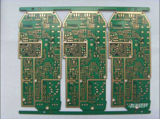
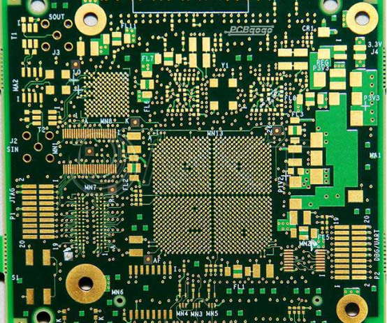
HDI stands for High Density Interconnector, a circuit board which has a relatively high line distribution density using the micro-blind and buried hole technology. It plays an important role in improving electrical performance and reducing the weight and the size of equipment.
There is a great demand on HDI PCB manufacturing with the development of technology and the many benefits HDI PCBs provide for high-tech applications. As a leading HDI printed circuit board supplier, PCBGOGO can offer you top-quality boards that have a significantly higher circuitry density with our specialized equipment and the capacity for advanced features, finer lines, and tighter tolerances.

HDI PCB, one of the fastest growing technologies in PCB industry. It includes blind and buried vias as well as microvias, which are .006 or less in diameter. There are 6 different kinds of HDI PCBs as the following:
Through vias from surface to surface
Buried vias and through vias
Two or more HDI layer with through vias
Passive substrate construction that have no electrical connection
Coreless construction with layer pairs
Alternative constructions of coreless builds with layer pairs
Consumer Driven Technology
The process of via-in-pad supports more technologies on fewer layers, bringing out that bigger is not always better. Since the late 1980's it can be seen that video cameras using cartridges the size of a novel, shrink to fit in the palm of your hand. it pushes technology further with the development of mobile computing and working from at home so that making computers faster and lighter, and allowing the consumer to work remotely from anywhere.
The main reason why it has these changes is that HDI technology. Do more products, less weight and smaller volume. Specialty equipment, mini-components and thinner materials have allowed for electronics to shrink in size while expanding technology, quality and speed.
Key HDI Benefits
The technology needs to change with the changing of consumer demands. Now designers have the options to place more components on both sides of the raw PCB by using HDI technology. And multiple via processes, including via in pad and blind via technology, allow designers to place components that are smaller even closer together for more PCB real estate.
The reduction of component size and pitch allow for more I/O in smaller geometries, which means faster transmission of signals and a signals and a significant reduction in signal loss and crossing delays.

Via in Pad Process
Since the late 1980's inspiration from surface mount technologies have pushed the limits BGA’s, COB and CSP into smaller square inches. The process of via in pad allows for vias to be placed within the surface of the flat lands. The via is plated and filled with either conductive or non-conductive epoxy then capped and plated over, making it virtually invisible.
It sounds simple but there is an average of eight additional steps to finish the special process. And trained technicians and speciality equipment should closely follow the process so that finish the perfect hidden via.
Via Fill Types
There are a lot of different kinds of via fill materials: conductive epoxy, non-conductive epoxy, silver filled, copper filled and electrochemical plating. These all lead to a via buried within a flat land that will completely solder as normal lands. It drills the vias and microvias, blind or buried, filled then plated and hidden beneath SMT lands. It needs to have the special equipment and wastes time on processing vias of this type. What’s more, it extends process time with the multiple drill cycles and controlled depth drilling.
Cost Effective HDI
While there are some consumer products reducing in size, quality is still the most important factor for the consumer second to price. It’s possible to reduce an 8 layer through-hole PCB to a 4 layer HDI microvia technology packed PCB with HDI technology in the design process. The wiring capabilities of a well-designed HDI 4 layer PCB can make it better as that of a standard 8 layer PCB.
The microvia process adds up to the cost of the HDI PCB, but the right design and reduction in layer count can reduce the cost in material square inches and layer count more significantly.
Building Non-Conventional HDI Boards
It needs to have special equipment and processes for successful manufacturing of HDI PCB, for example, plugging, laser drills, laser direct imaging and sequential lamination cycles. HDI PCB has tighter spacing, tighter annular ring and thinner lines. So it needs to additional time and a significant investment in manufacturing processes and equipment for this kinds of board that to be fabricated successfully.
Laser Drill Technology
It can allow for more technologies on the PCB surface for drilling the smallest of microvias. The high influence beam can cut through metal and glass to create the tiny via hole with a beam of light 20 microns ( 1 Mil ) in diameter. There are new products such as uniform glass materials that are a low loss laminate and low dielectric constant. These materials have higher heat resistance than lead free assembly and allow for the smaller holes to be used.
Lamination & Materials For HDI Boards
Advanced multilayer technology allows for designers to add additional pairs of layers to make a multilayer PCB in turns. There is a process called sequential build up, which produces holes in the internal layers with the use of a laser drill to be plating, imaging and etching prior to pressing. It can have a better thermal management, a stronger inter connect and increasing the board's reliability as SBU fabrication uses solid plug hole.
It develops specifically the resin coated copper to aide with longer drill times, poor hole quality and to allow for thinner PCBs. RCC has an ultra-thin copper foil and ultra-low profile that is anchored with minuscule nodules to the surface. The material can be the thinnest and finest line and spacing technology after treating chemically and priming.
The application of dry resist to the laminate still uses heated roll method to apply the resist to core material. Now it’s recommended to preheat the material to a desired temperature before teh lamination process for HDI PCB. The preheating of material makes the dry resist do well in sticking to the surface of the laminate, pulling less heat away from the hot rolls and allowing for consistent stable exit temperatures of the laminated product. It’s important to the reproduction of fine lines and spacing as consistent entrance and exit temperatures result in less air entrapment beneath the film.
LDI & Contact Imagery
It’s expensive but necessary to use semiconductor Class 100 Clean rooms to process these HDI parts process these HDI parts and image finer lines than ever before. And it needs to have much tighter controls for spacing, finer lines and annular ring, touch up rework or repair becomes an impossible task with use of finer lines. There are some necessary factors for successful process, for example, photo tool quality, laminate prep and imaging parameters. It can reduce defects with a clean room atmosphere, and dry film resist is still the number one process for all technology boards.
There is a widely used for contact imaging because of the cost of laser direct imaging, but for such fine lines and spacing, LDI is a far better option. Now a lot of factories still use contact imaging in a SC100 room. With the demand expands, there is a increasing demand on laser drilling and laser direct imaging. So HDI production facilities in PCBGOGO fabricate the HDI PCB with the latest in technology equipment.
There are some products pushing technology to smaller and lighter requirements for the consumer’s daily use, such as cameras, laptops, scanners and cell phones. In 1992, the averages cell phone weighted 220-250 grams has the limits of making phone calls. But now we call, surf the net, text, play our favorite songs or games take pictures and videos on one tiny device weighing 151 grams. So it pushes HDI technology with current changing culture, and PCBGOGO will be here to help you if you have any questions.

Why Choose PCBGOGO?
With over 10 years, PCBGOGO not only highly specialized in quick-turn PCB fabrication and assembly, but also high-density interconnect PCB fabrication. we are committed to adhering to the strictest standards in PCB manufacturing and assembly with four guarantees, such as PCB material guaranteed, quality guaranteed, on-time shipping guaranteed, and reasonable guaranteed. So you will have a winning combination for all your HDI PCB needs with competitive price, quick quotes and response times.
Get a instant quote today to learn more about our high-quality, cost-effective services.
- Comments(0)
