日本語
 한국어

Why Multilayer PCB Copper Balancing Cannot Be Ignored?90% of Engineers Fall into These Traps
Multilayer PCB warpage, delamination after lamination, and yield drops in mass production are among the most common complaints engineers raise during PCB manufacturing. After repeated root-cause analysis, one issue frequently emerges as the hidden culprit: poor copper balancing.
Many engineers still regard copper balancing as a minor layout detail. In reality, it has a direct and measurable impact on PCB mechanical stability, lamination reliability, and electrical performance, especially for high-layer-count and high-density designs. This article explains what copper balancing is, why it matters, and the most common mistakes engineers make.
What Is Copper Balancing in Multilayer PCBs?
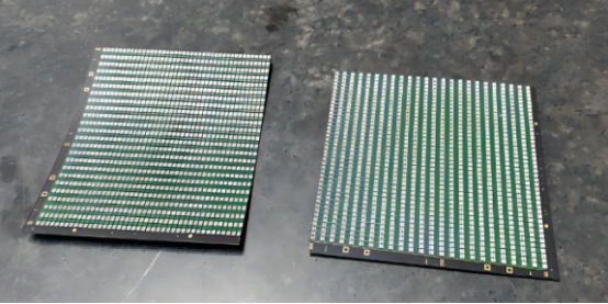
Copper balancing refers to maintaining a relatively uniform copper area and distribution across each PCB layer, particularly between symmetrical layers (such as top vs. bottom layers, or L2 vs. L5 in an 8-layer stack-up).
A multilayer PCB can be compared to a sandwich: each copper layer acts as a filling. If one side contains significantly more copper than the other, uneven heating and stress during lamination will cause the board to warp or deform.
Industry Reference Guidelines
Copper area difference between symmetrical layers: ≤ 10% recommended
Differences above 15% significantly increase warpage risk
Overall board copper coverage: 40%–70% is optimal for lamination stability
Based on PCBGOGO production data, copper imbalance accounts for approximately 30% of multilayer PCB defects, particularly in designs with 6 layers or more, where stress accumulation becomes more pronounced.
Three Critical Impacts of Copper Imbalance in Multilayer PCBs
Ignoring copper balance does not just cause cosmetic defects—it directly affects manufacturability and long-term reliability.
1. PCB Warpage After Lamination and Assembly Failure
This is the most frequently observed consequence.
In one 8-layer industrial control PCB, the top layer copper coverage was 25%, while the bottom layer reached 55%. After lamination, board warpage exceeded 0.8 mm, preventing assembly into the enclosure and forcing full batch rework.
As copper imbalance increases, lamination stress becomes more concentrated, leading not only to warpage but, in severe cases, cracking.
2. Delamination and Blistering, Resulting in Poor Reliability
Copper and substrate materials have different coefficients of thermal expansion (CTE). When copper distribution is uneven, layers shrink inconsistently during lamination, creating internal stress.
During soldering or field use, thermal cycling releases this stress, causing:
Interlayer delamination
Blistering and bubble formation
PCBGOGO laboratory testing shows that multilayer boards with unbalanced copper distribution exhibit a delamination rate four times higher than balanced boards after 85°C / 85% RH damp heat aging tests.
3. Unstable Electrical Performance and Impedance Variation
Copper imbalance also affects signal integrity, especially in high-frequency multilayer PCBs.
Uneven copper distribution in signal layers can cause characteristic impedance deviations exceeding ±5%, resulting in:
Increased signal reflection
Higher crosstalk
Large fluctuations in test data
Failure to meet performance specifications
Three Common Copper Balancing Pitfalls Engineers Often Overlook
Pitfall 1: Focusing Only on Total Copper Area, Ignoring Local Distribution
Some designers assume that similar total copper percentages are sufficient. However, local copper concentration matters.
For example, if the top layer contains a large 20 mm × 30 mm copper pour while the bottom layer consists of evenly distributed fine traces, local stress imbalance during lamination can still cause warpage.
Pitfall 2: Random Copper Addition That Backfires
When copper coverage is insufficient, some engineers add isolated copper patches arbitrarily. These floating copper islands:
Do not improve stress balance
Have poor adhesion to the substrate
Easily form bubbles after lamination
Effective copper balancing requires continuous copper connection, typically tied to ground or power planes, often in a mesh pattern.
Pitfall 3: Ignoring Copper Balance in Inner Layers
Many designs focus only on the top and bottom layers while overlooking inner layers such as L2 and L3. However, multilayer boards are laminated as a whole.
Copper imbalance in the inner layers also generates internal stress, ultimately leading to overall board deformation. During PCBGOGO’s DFM reviews, copper distribution is checked across all layers, not just the outer ones.
Practical Recommendations for Achieving Proper Copper Balance
Achieving copper balance does not require complex techniques—only disciplined design practices.
1. Evaluate Copper Area During the Design Stage
Use the copper area statistics function in PCB design software. After completing each layer:
Compare it with its symmetrical counterpart
If the difference exceeds 10%, adjust accordingly
Common methods include adding grid copper pours in low-coverage areas or opening windows in high-coverage zones, provided electrical performance is unaffected.
2. Ensure Continuous Copper Connection
Added copper should not be isolated. Recommended practices include:
Connecting copper pours to ground or power planes
Using mesh copper patterns
Grid spacing is typically 0.8–1.2 mm, which increases copper area without compromising heat dissipation or signal integrity
3. Submit Designs for DFM Review
If the copper balance is uncertain, submitting the design for a DFM (Design for Manufacturability) review can prevent costly production issues.
PCBGOGO engineers use professional analysis tools to evaluate copper distribution on every layer and provide specific, actionable recommendations on where to add or remove copper before mass production.
Conclusion: Copper Balancing Is a Design Discipline, Not an Afterthought
Copper balancing in multilayer PCBs is neither mysterious nor optional. It is a foundational design discipline that directly affects lamination quality, mechanical stability, signal integrity, and production yield.
Rather than addressing warpage, delamination, and rework after production begins, investing time in proper copper balancing during the design phase saves cost and ensures consistent product quality. For complex multilayer designs, experienced manufacturers like PCBGOGO can help engineers avoid common pitfalls through early-stage technical review and proven manufacturing expertise.